You can not select more than 25 topics
Topics must start with a letter or number, can include dashes ('-') and can be up to 35 characters long.
3.6 KiB
3.6 KiB
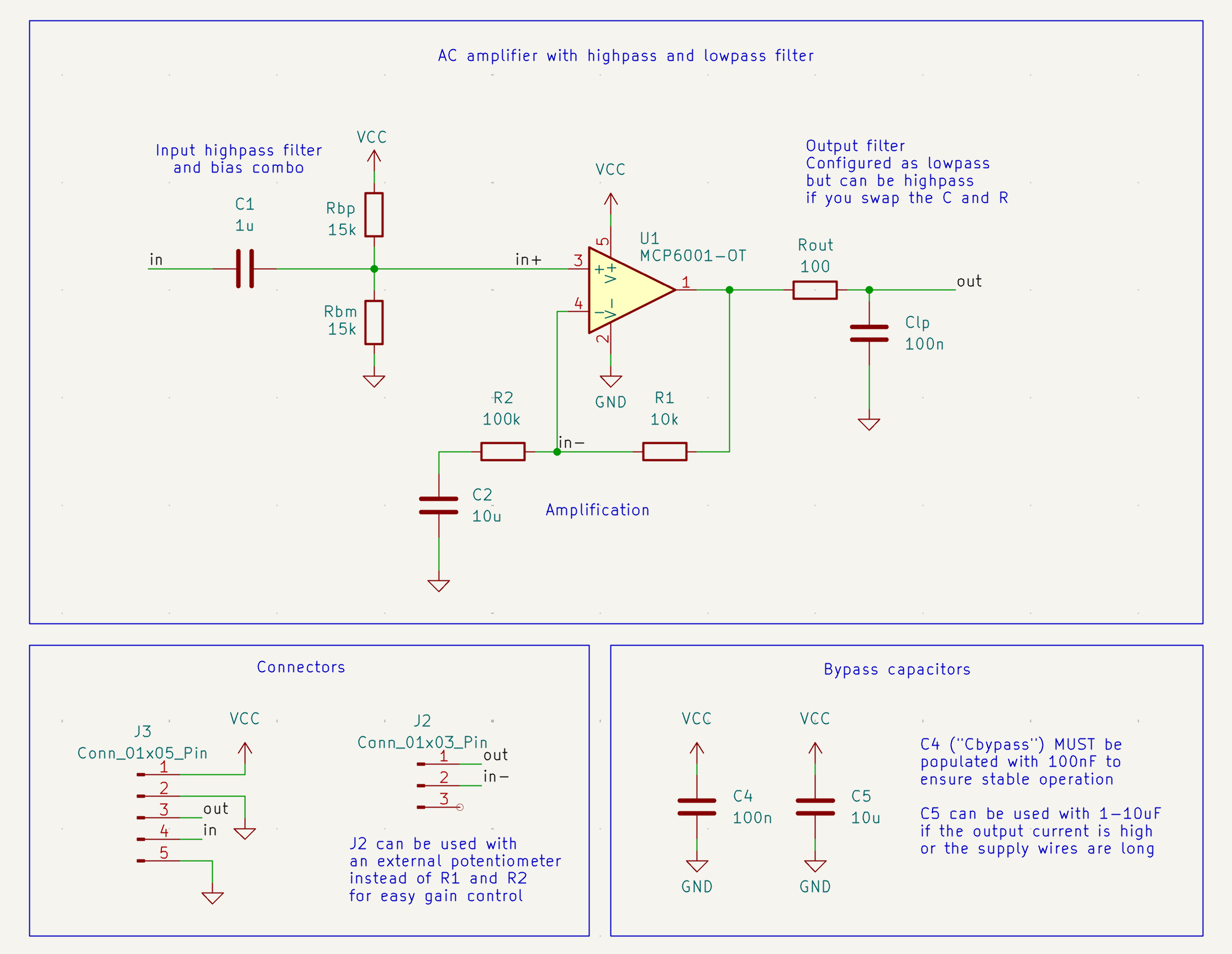
Op-Amp AC amplifier with highpass and lowpass filters
- For use with MCP6001 or similar amplifier
- Works with mV inputs centered around GND
- Few components, 0603 passives for easy soldering

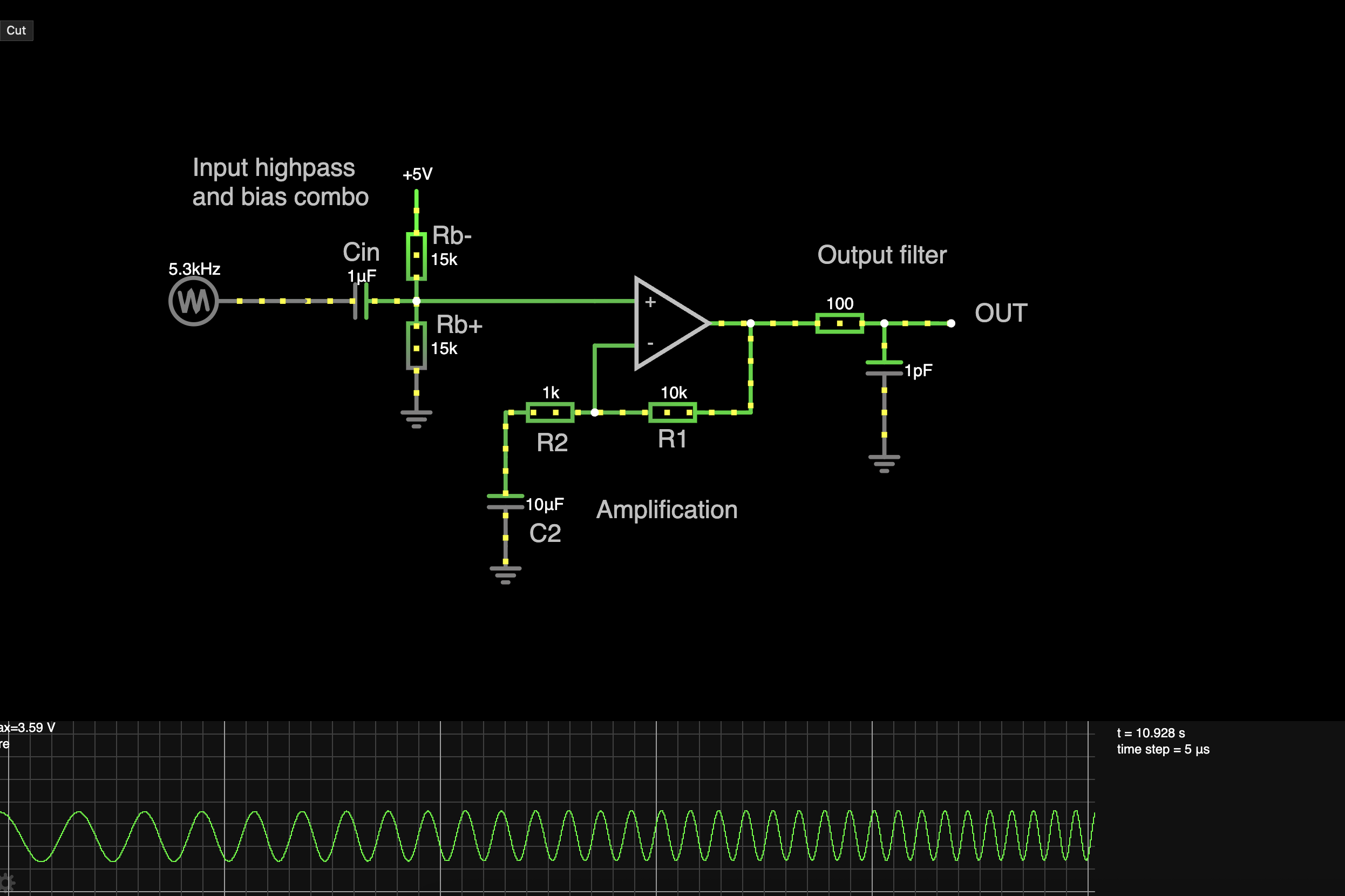
Basic configuration
Behaviour:
- 11x gain
- Bandpass 20Hz - 15kHz (approx, not textbook perfect!)
- Vcc 3-5V
- Makes 10mV signal centered around GND into a 110mV signal centered around 2.5V
- Output centered arround VCC/2
- To directly drive headphones you must add a DC blocking capacitor! (between OUT and your headphones, 100uF should be fine)
Easy adjustments for people in a hurry:
- More gain? -> Increase R2 with respect to R1
- Pass higher frequencies? -> Reduce Clp or Rout (or both)
- Pass lower frequencies? -> Increase both Rb+ and Rb- (same value!)
- Lower center voltage of output? -> Increase Rb+ relative to Rb-
- Achive the opposite of any of the above? -> Do the opposite of any of the above
Note! The MCP6001 has a GBW of 1MHz. This means, if the gain is set to 100x, the amplifier will drop 3dB at 1MHz/100x = 10kHz! For very low input frequencies (<5Hz), you may need to increase C1 and C2.
Design details
C1, Rb+ and Rb- together form a combo bias and highpass filter
- Since the op-amp does not have a negative voltage rail, the signal can not be less than GND
- Therefore, the input must be biased - pulled towards some positive voltage
- If Rb+ = Rb-, then the bias will be VCC/2 - the signal will be centered around VCC/2
- Adjusting them relative to eachother allows you to pick a different center voltage
- The parallel resistance of Rb+ and Rb-, together with C1 forms a HIGHPASS FILTER
- Increasing the resistance lowers the pass frequency
R1 and R2 set the gain
- Gain = R2/R1 + 1
- Gain is limited by the GBW (gain-bandwidth product) of the op-amp used
- MCP6001 has a GBW of 1MHz, so max frequency = 1MHz / gain (3db loss at that frequency)
C2 makes the output centered around the biasing frequency
- Whatever voltage Rb+ and Rb- form, will be the center frequency of the output
- In essance, the gain for DC is 0 (since the gain resistors R1 and R2 have not DC path to GND)
- C2 just needs to be big enough, when it is big enough it does not affect filtering
Rlp and Cout can be used for an output lowpass
- Classic low pass filter, nothing to see here
Rlp and Cout can instead be used for an output highpass
- Just swap the position of the capacitor and resistor. It's ok, they fit.
Soldering tips

- Solder under the stereo optical microscope
- Start with the Op-amp
- Then the resistors and capacitors
- Last the pin header
- If you make the pins face down, the PCB looks cool on a breadboard
- If you make the pins face up, its easy to re-work the soldering